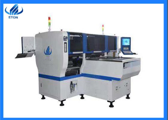
HT-E8D machine is Dual system,dual module multifunctional mounter with high capacity of 80000CPH. It can mount capacitors,resistors,LED3014/3020/3528/5050,IC and shaped components. It applies to power driver,electric board,lens,linear bulb,household appliance and etc..
6.Company profile

7.Our clients
8.FAQ
SMT Patch Process
Incoming inspection => screen printing solder paste (spotting glue)=> patch => drying (curing)=> reflux welding => cleaning inspection => rework
A: incoming inspection =>PCB A surface silk-screen solder paste (dot patch glue)=>PCB> patch PCB surface silk-screen solder paste (dot patch glue). patch =>PCB> drying and reflow welding (preferably only for B surface cleaning =>PCB> detection and rework).
B: incoming inspection =>PCB A surface silk-screen solder paste (spotting glue)=>PCB> patch drying (curing)=>PCB> A surface reflow welding cleaning =>PCB> flip-flop =>PCB =>PCB=>PCB> surface spotting glue/patch curing =>PCB> surface wave soldering inspection and rework)
This process is suitable for PCB A surface reflux welding, B surface wave peak welding. this process is appropriate in PCB SMD assembled on the B surface only if SOT or below the pin.
- Single side mixing process:
A surface silkscreen solder paste (spotting glue)=>PCB> patch =>PCB> drying (curing)=>PCB> reflow soldering =>PCB> cleaning plug-in =>PCB> wave soldering inspection =>PCB> re-repair
- Double-sided mixing process:
B surface patch glue =>PCB> patch =>PCB> curing =>PCB> flip =>PCB =>PCB> wave soldering =>PCB> cleaning and inspection repair
Apply to SMD more than separate components
A surface plug-in (pin bending) B: incoming inspection =>PCB =>PCB> B surface spot patch glue =>PCB> patch cured flip-flop =>PCB> wave soldering inspection and repair
First insert and then paste, suitable for separating components more than SMD components
C: incoming inspection =>PCB A surface silk-screen solder paste =>PCB> patch drying =>PCB> reflux welding plug-in, pin bending =>PCB> flip-flop =>PCB of the B surface spot patch glue, patch curing =>PCB> flip-flop wave soldering cleaning detection =>PCB> rework surface mixed, B surface mount.
D: incoming inspection =>PCB B surface spot patch glue =>PCB> patch cured =>PCB> flip-flop =>PCB A surface silk-screen solder paste patch surface reflow welding plug-in =>PCB> B surface wave soldering cleaning detection =>PCB> rework surface mixing, surface mount. B surface silk-screen solder paste (spotting glue)==>PCB patch ==>PCB drying (curing)==>PCB A surface silk-screen solder paste =>PCB reflow soldering, patch drying = reflow soldering 1(local welding can be used), plug-in, wave soldering 2(if insert components are few ==>PCB, Manual welding can be used)==>PCB cleaning ==>PCB testing ==>PCB rework A surface mount, B surface mix.
- Double-sided assembly process
A: incoming inspection, PCB A silk-screen solder paste (patch glue), patch, drying (curing), A surface reflow welding, cleaning, flip plate; PCB silk-screen solder paste (patch glue), patch, drying, reflow welding (preferably only for B surface, cleaning, testing, rework)
This process is suitable for PCB with large SMD such as PLCC on both sides.
B: incoming inspection, PCB A surface silk-screen solder paste (spot patch glue), patch, drying (curing), A surface reflow welding, cleaning, flip plate; PCB surface spot patch glue, patch, curing, B surface wave soldering, cleaning, testing, rework) this process is suitable for reflow on PCB surface.
contact
Name:Brynn
Email :Brynn@eton-mounter.com
WeChat:13802252825
Telephone:138 0225 2825

 आपका संदेश 20-3,000 अक्षरों के बीच होना चाहिए!